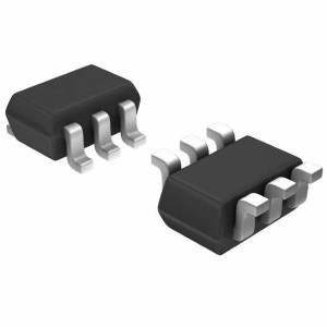
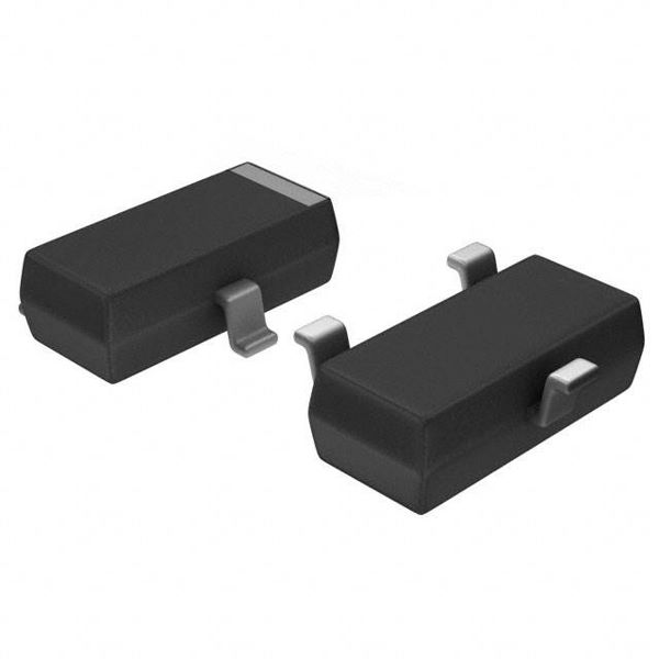
FDV301N MOSFET N-Ch Digital
♠ Product Description
| Product Attribute | Attribute Value |
| Manufacturer: | onsemi |
| Product Category: | MOSFET |
| RoHS: | Details |
| Technology: | Si |
| Mounting Style: | SMD/SMT |
| Package / Case: | SOT-23-3 |
| Transistor Polarity: | N-Channel |
| Number of Channels: | 1 Channel |
| Vds - Drain-Source Breakdown Voltage: | 25 V |
| Id - Continuous Drain Current: | 220 mA |
| Rds On - Drain-Source Resistance: | 5 Ohms |
| Vgs - Gate-Source Voltage: | - 8 V, + 8 V |
| Vgs th - Gate-Source Threshold Voltage: | 700 mV |
| Qg - Gate Charge: | 700 pC |
| Minimum Operating Temperature: | - 55 C |
| Maximum Operating Temperature: | + 150 C |
| Pd - Power Dissipation: | 350 mW |
| Channel Mode: | Enhancement |
| Packaging: | Reel |
| Packaging: | Cut Tape |
| Packaging: | MouseReel |
| Brand: | onsemi / Fairchild |
| Configuration: | Single |
| Fall Time: | 6 ns |
| Forward Transconductance - Min: | 0.2 S |
| Height: | 1.2 mm |
| Length: | 2.9 mm |
| Product: | MOSFET Small Signal |
| Product Type: | MOSFET |
| Rise Time: | 6 ns |
| Series: | FDV301N |
| Factory Pack Quantity: | 3000 |
| Subcategory: | MOSFETs |
| Transistor Type: | 1 N-Channel |
| Type: | FET |
| Typical Turn-Off Delay Time: | 3.5 ns |
| Typical Turn-On Delay Time: | 3.2 ns |
| Width: | 1.3 mm |
| Part # Aliases: | FDV301N_NL |
| Unit Weight: | 0.000282 oz |
♠ Digital FET, N-Channel FDV301N, FDV301N-F169
This N−Channel logic level enhancement mode field effect transistor is produced using onsemi’s proprietary, high cell density, DMOS technology. This very high density process is especially tailored to minimize on−state resistance. This device has been designed especially for low voltage applications as a replacement for digital transistors. Since bias resistors are not required, this one N−channel FET can replace several different digital transistors, with different bias resistor values.
• 25 V, 0.22 A Continuous, 0.5 A Peak
♦ RDS(on) = 5 @ VGS = 2.7 V
♦ RDS(on) = 4 @ VGS = 4.5 V
• Very Low Level Gate Drive Requirements Allowing Direct Operation in 3 V Circuits. VGS(th) < 1.06 V
• Gate−Source Zener for ESD Ruggedness. > 6 kV Human Body Model
• Replace Multiple NPN Digital Transistors with One DMOS FET
• This Device is Pb−Free and Halide Free