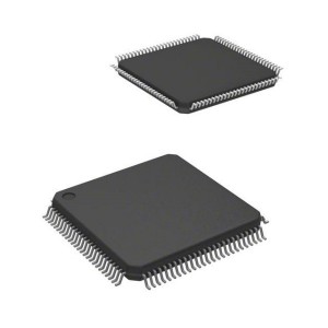
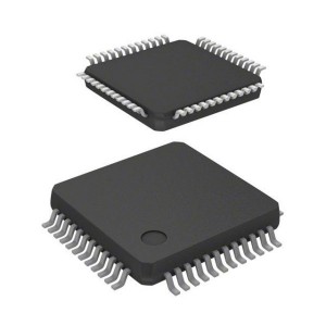
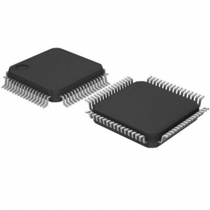
LCMXO2-4000HC-4TG144C Field Programmable Gate Array 4320 LUTs 115 IO 3.3V 4 Spd
♠ Product Description
| Product Attribute | Attribute Value |
| Manufacturer: | Lattice |
| Product Category: | FPGA - Field Programmable Gate Array |
| RoHS: | Details |
| Series: | LCMXO2 |
| Number of Logic Elements: | 4320 LE |
| Number of I/Os: | 114 I/O |
| Supply Voltage - Min: | 2.375 V |
| Supply Voltage - Max: | 3.6 V |
| Minimum Operating Temperature: | 0 C |
| Maximum Operating Temperature: | + 85 C |
| Data Rate: | - |
| Number of Transceivers: | - |
| Mounting Style: | SMD/SMT |
| Package / Case: | TQFP-144 |
| Packaging: | Tray |
| Brand: | Lattice |
| Distributed RAM: | 34 kbit |
| Embedded Block RAM - EBR: | 92 kbit |
| Maximum Operating Frequency: | 269 MHz |
| Moisture Sensitive: | Yes |
| Number of Logic Array Blocks - LABs: | 540 LAB |
| Operating Supply Current: | 8.45 mA |
| Operating Supply Voltage: | 2.5 V/3.3 V |
| Product Type: | FPGA - Field Programmable Gate Array |
| Factory Pack Quantity: | 60 |
| Subcategory: | Programmable Logic ICs |
| Total Memory: | 222 kbit |
| Tradename: | MachXO2 |
| Unit Weight: | 0.046530 oz |
1. Flexible Logic Architecture
Six devices with 256 to 6864 LUT4s and 18 to 334 I/O
2. Ultra Low Power Devices
Advanced 65 nm low power process
As low as 22 μW standby power
Programmable low swing differential I/O
Stand-by mode and other power saving options
3. Embedded and Distributed Memory
Up to 240 kbits sysMEM™ Embedded Block RAM
Up to 54 kbits Distributed RAM
Dedicated FIFO control logic
4. On-Chip User Flash Memory
Up to 256 kbits of User Flash Memory
100,000 write cycles
Accessible through WISHBONE, SPI, I2C and JTAG interfaces
Can be used as soft processor PROM or as Flash memory
5. Pre-Engineered Source Synchronous I/O
DDR registers in I/O cells
Dedicated gearing logic
7:1 Gearing for Display I/O
Generic DDR, DDRX2, DDRX4
Dedicated DDR/DDR2/LPDDR memory with DQS support
6. High Performance, Flexible I/O Buffer
Programmable sysI/O™ buffer supports wide range of interfaces:
LVCMOS 3.3/2.5/1.8/1.5/1.2
LVTTL
PCI
LVDS, Bus-LVDS, MLVDS, RSDS, LVPECL
SSTL 25/18
HSTL 18
MIPI D-PHY Emulated
Schmitt trigger inputs, up to 0.5 V hysteresis
I/O support hot socketing
On-chip differential termination
Programmable pull-up or pull-down mode
7. Flexible On-Chip Clocking
Eight primary clocks
Up to two edge clocks for high-speed I/O interfaces (top and bottom sides only)
Up to two analog PLLs per device with fractional-n frequency synthesis
Wide input frequency range (7 MHz to 400 MHz)
8. Non-volatile, Infinitely Reconfigurable
Instant-on – powers up in microseconds
Single-chip, secure solution
Programmable through JTAG, SPI or I2C
Supports background programming of non-volatile memory
Optional dual boot with external SPI memory
9. TransFR™ Reconfiguration
In-field logic update while system operates
10. Enhanced System Level Support
On-chip hardened functions: SPI, I2C, timer/counter
On-chip oscillator with 5.5% accuracy
Unique TraceID for system tracking
One Time Programmable (OTP) mode
Single power supply with extended operating range
IEEE Standard 1149.1 boundary scan
IEEE 1532 compliant in-system programming
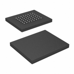
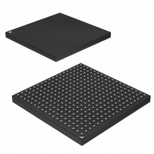
11. Broad Range of Package Options
TQFP, WLCSP, ucBGA, csBGA, caBGA, ftBGA, fpBGA, QFN package options
Small footprint package options
As small as 2.5 mm x 2.5 mm
Density migration supported
Advanced halogen-free packaging