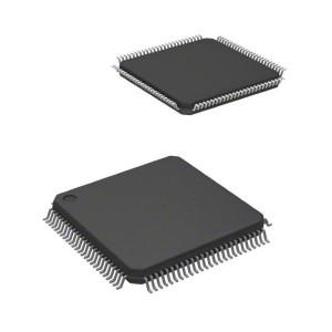
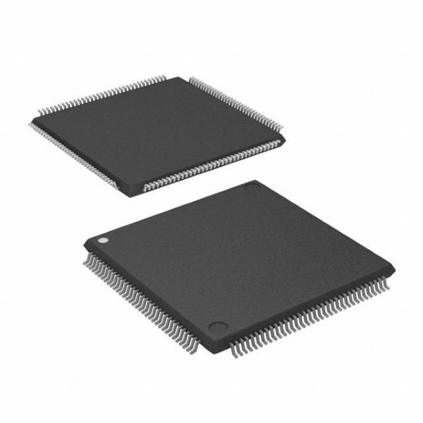
LCMXO640C-3TN144I FPGA – Field Programmable Gate Array 640 LUTS 113 I/0
♠ Product Description
| Product Attribute | Attribute Value |
| Manufacturer: | Lattice |
| Product Category: | FPGA - Field Programmable Gate Array |
| RoHS: | Details |
| Series: | LCMXO640C |
| Number of Logic Elements: | 640 LE |
| Number of I/Os: | 113 I/O |
| Supply Voltage - Min: | 1.71 V |
| Supply Voltage - Max: | 3.465 V |
| Minimum Operating Temperature: | - 40 C |
| Maximum Operating Temperature: | + 100 C |
| Data Rate: | - |
| Number of Transceivers: | - |
| Mounting Style: | SMD/SMT |
| Package/Case: | TQFP-144 |
| Packaging: | Tray |
| Brand: | Lattice |
| Distributed RAM: | 6.1 kbit |
| Height: | 1.4 mm |
| Length: | 20 mm |
| Maximum Operating Frequency: | 500 MHz |
| Moisture Sensitive: | Yes |
| Number of Logic Array Blocks - LABs: | 80 LAB |
| Operating Supply Current: | 17 mA |
| Operating Supply Voltage: | 1.8 V/2.5 V/3.3 V |
| Product Type: | FPGA - Field Programmable Gate Array |
| Factory Pack Quantity: | 60 |
| Subcategory: | Programmable Logic ICs |
| Total Memory: | 6.1 kbit |
| Width: | 20 mm |
| Unit Weight: | 1.319 g |
Non-volatile, Infinitely Reconfigurable
• Instant-on – powers up in microseconds
• Single chip, no external configuration memory required
• Excellent design security, no bit stream to intercept
• Reconfigure SRAM based logic in milliseconds
• SRAM and non-volatile memory programmable through JTAG port
• Supports background programming of non-volatile memory
Sleep Mode
• Allows up to 100x static current reduction
TransFR™ Reconfiguration (TFR)
• In-field logic update while system operates
High I/O to Logic Density
• 256 to 2280 LUT4s
• 73 to 271 I/Os with extensive package options
• Density migration supported
• Lead free/RoHS compliant packaging
Embedded and Distributed Memory
• Up to 27.6 Kbits sysMEM™ Embedded Block RAM
• Up to 7.7 Kbits distributed RAM
• Dedicated FIFO control logic
Flexible I/O Buffer
• Programmable sysIO™ buffer supports wide range of interfaces:
– LVCMOS 3.3/2.5/1.8/1.5/1.2
– LVTTL
– PCI
– LVDS, Bus-LVDS, LVPECL, RSDS
sysCLOCK™ PLLs
• Up to two analog PLLs per device
• Clock multiply, divide, and phase shifting
System Level Support
• IEEE Standard 1149.1 Boundary Scan
• Onboard oscillator
• Devices operate with 3.3V, 2.5V, 1.8V or 1.2V power supply
• IEEE 1532 compliant in-system programming