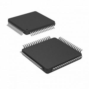
LPC2468FBD208 Microcontroladores ARM – MCU Single-chip 16-bit/32-bit micro;

♠ Product Description
| Atributo del producto | Valor de atributo |
| Fabricante: | NXP |
| Categoría de producto: | Microcontroladores ARM - MCU |
| RoHS: | Detalles |
| Estilo de montaje: | SMD/SMT |
| Núcleo: | ARM7TDMI-S |
| Tamaño de memoria del programa: | 512 kB |
| Ancho de bus de datos: | 32 bit/16 bit |
| Resolución del conversor de señal analógica a digital (ADC): | 10 bit |
| Frecuencia de reloj máxima: | 72 MHz |
| Número de entradas / salidas: | 160 I/O |
| Tamaño de RAM de datos: | 98 kB |
| Voltaje de alimentación - Mín.: | 3.3 V |
| Voltaje de alimentación - Máx.: | 3.3 V |
| Temperatura de trabajo mínima: | - 40 C |
| Temperatura de trabajo máxima: | + 85 C |
| Empaquetado: | Tray |
| Marca: | NXP Semiconductors |
| Sensibles a la humedad: | Yes |
| Tipo de producto: | ARM Microcontrollers - MCU |
| Cantidad de empaque de fábrica: | 180 |
| Subcategoría: | Microcontrollers - MCU |
| Alias de las piezas n.º: | 935282457557 |
♠LPC2468 Single-chip 16-bit/32-bit micro; 512 kB flash, Ethernet, CAN, ISP/IAP, USB 2.0 device/host/OTG, external memory interface
NXP Semiconductors designed the LPC2468 microcontroller around a 16-bit/32-bit ARM7TDMI-S CPU core with real-time debug interfaces that include both JTAG and embedded trace. The LPC2468 has 512 kB of on-chip high-speed flash memory.
This flash memory includes a special 128-bit wide memory interface and accelerator architecture that enables the CPU to execute sequential instructions from flash memory at the maximum 72 MHz system clock rate. This feature is available only on the LPC2000 ARM microcontroller family of products.
The LPC2468 can execute both 32-bit ARM and 16-bit Thumb instructions. Support for the two instruction sets means engineers can choose to optimize their application for either performance or code size at the sub-routine level. When the core executes instructions in Thumb state it can reduce code size by more than 30 % with only a small loss in performance while executing instructions in ARM state maximizes core performance.
The LPC2468 microcontroller is ideal for multi-purpose communication applications. It incorporates a 10/100 Ethernet Media Access Controller (MAC), a USB full-speed Device/Host/OTG Controller with 4 kB of endpoint RAM, four UARTs, two Controller Area Network (CAN) channels, an SPI interface, two Synchronous Serial Ports (SSP), three I2C interfaces, and an I2S interface. Supporting this collection of serial communications interfaces are the following feature components; an on-chip 4 MHz internal precision oscillator, 98 kB of total RAM consisting of 64 kB of local SRAM, 16 kB SRAM for Ethernet, 16 kB SRAM for general purpose DMA, 2 kB of battery powered SRAM, and an External Memory Controller (EMC).
These features make this device optimally suited for communication gateways and protocol converters. Complementing the many serial communication controllers, versatile clocking capabilities, and memory features are various 32-bit timers, an improved 10-bit ADC, 10-bit DAC, two PWM units, four external interrupt pins, and up to 160 fast GPIO lines.
The LPC2468 connects 64 of the GPIO pins to the hardware based Vector Interrupt Controller (VIC) that means these external inputs can generate edge-triggered interrupts. All of these features make the LPC2468 particularly suitable for industrial control and medical systems.
ARM7TDMI-S processor, running at up to 72 MHz.
512 kB on-chip flash program memory with In-System Programming (ISP) and In-Application Programming (IAP) capabilities. Flash program memory is on the ARM local bus for high performance CPU access.
98 kB on-chip SRAM includes:
64 kB of SRAM on the ARM local bus for high performance CPU access.
16 kB SRAM for Ethernet interface. Can also be used as general purpose SRAM.
16 kB SRAM for general purpose DMA use also accessible by the USB.
2 kB SRAM data storage powered from the Real-Time Clock (RTC) power domain.
Dual Advanced High-performance Bus (AHB) system allows simultaneous Ethernet DMA, USB DMA, and program execution from on-chip flash with no contention.
EMC provides support for asynchronous static memory devices such as RAM, ROM and flash, as well as dynamic memories such as single data rate SDRAM.
Advanced Vectored Interrupt Controller (VIC), supporting up to 32 vectored interrupts.
General Purpose DMA controller (GPDMA) on AHB that can be used with the SSP, I 2S-bus, and SD/MMC interface as well as for memory-to-memory transfers.
Serial Interfaces:
Ethernet MAC with MII/RMII interface and associated DMA controller. These functions reside on an independent AHB.
USB 2.0 full-speed dual port device/host/OTG controller with on-chip PHY and associated DMA controller.
Four UARTs with fractional baud rate generation, one with modem control I/O, one with IrDA support, all with FIFO.
CAN controller with two channels.
SPI controller.
Two SSP controllers, with FIFO and multi-protocol capabilities. One is an alternate for the SPI port, sharing its interrupt. SSPs can be used with the GPDMA controller.
Three I2C-bus interfaces (one with open-drain and two with standard port pins).
I 2S (Inter-IC Sound) interface for digital audio input or output. It can be used with the GPDMA.
Other peripherals:
SD/MMC memory card interface.
160 General purpose I/O pins with configurable pull-up/down resistors.
10-bit ADC with input multiplexing among 8 pins.
10-bit DAC.
Four general purpose timers/counters with 8 capture inputs and 10 compare outputs. Each timer block has an external count input.
Two PWM/timer blocks with support for three-phase motor control. Each PWM has an external count inputs.
RTC with separate power domain. Clock source can be the RTC oscillator or the APB clock.
2 kB SRAM powered from the RTC power pin, allowing data to be stored when the rest of the chip is powered off.
WatchDog Timer (WDT). The WDT can be clocked from the internal RC oscillator, the RTC oscillator, or the APB clock.
Standard ARM test/debug interface for compatibility with existing tools.
Emulation trace module supports real-time trace.
Single 3.3 V power supply (3.0 V to 3.6 V).
Four reduced power modes: idle, sleep, power-down, and deep power-down.
Four external interrupt inputs configurable as edge/level sensitive. All pins on port 0 and port 2 can be used as edge sensitive interrupt sources.
Processor wake-up from Power-down mode via any interrupt able to operate during Power-down mode (includes external interrupts, RTC interrup,USB activity, Ethernet wake-up interrupt, CAN bus activity, port 0/2 pin interrupt). Two independent power domains allow fine tuning of power consumption based on needed features.
Each peripheral has its own clock divider for further power saving. These dividers help reduce active power by 20 % to 30 %.
Brownout detect with separate thresholds for interrupt and forced reset.
On-chip power-on reset. On-chip crystal oscillator with an operating range of 1 MHz to 25 MHz.
4 MHz internal RC oscillator trimmed to 1 % accuracy that can optionally be used as the system clock. When used as the CPU clock, does not allow CAN and USB to run.
On-chip PLL allows CPU operation up to the maximum CPU rate without the need for a high frequency crystal. May be run from the main oscillator, the internal RC oscillator, or the RTC oscillator.
Boundary scan for simplified board testing.
Versatile pin function selections allow more possibilities for using on-chip peripheral functions.
Industrial control
Medical systems
Protocol converter
Communications