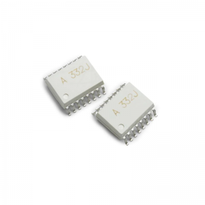
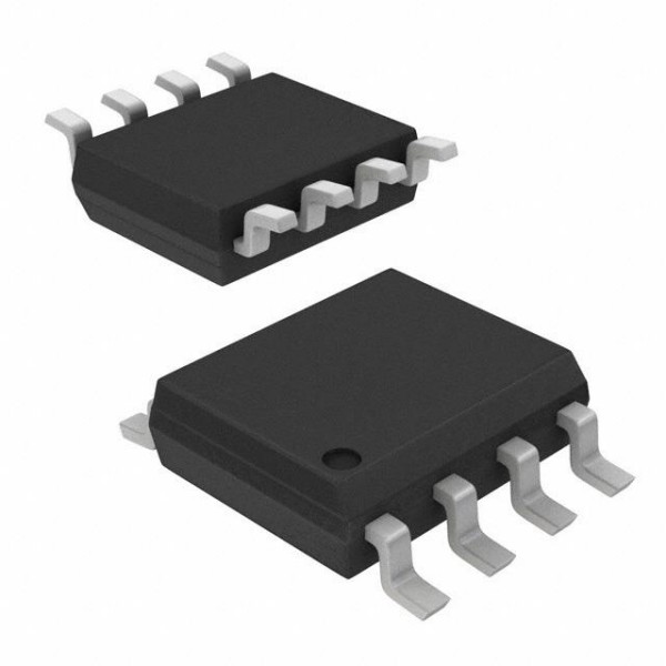
MOCD217R2M Transistor Output Optocouplers SO-8 OPTOC. DUAL CH
♠ Product Description
| Product Attribute | Attribute Value |
| Manufacturer: | onsemi |
| Product Category: | Transistor Output Optocouplers |
| Mounting Style: | SMD/SMT |
| Package / Case: | SOIC-Narrow-8 |
| Number of Channels: | 2 Channel |
| Isolation Voltage: | 2500 Vrms |
| Output Type: | NPN Phototransistor |
| Current Transfer Ratio: | 100 % |
| If - Forward Current: | 60 mA |
| Vf - Forward Voltage: | 1.3 V |
| Maximum Collector Emitter Voltage: | 30 V |
| Maximum Collector Current: | 150 mA |
| Maximum Collector Emitter Saturation Voltage: | 0.4 V |
| Rise Time: | 3.2 us |
| Fall Time: | 4.7 us |
| Vr - Reverse Voltage: | 6 V |
| Pd - Power Dissipation: | 240 mW |
| Minimum Operating Temperature: | - 40 C |
| Maximum Operating Temperature: | + 100 C |
| Series: | MOCD217M |
| Packaging: | Reel |
| Packaging: | Cut Tape |
| Packaging: | MouseReel |
| Brand: | onsemi / Fairchild |
| Configuration: | 2 Channel |
| Height: | 3.43 mm |
| Length: | 5.13 mm |
| Product Type: | Transistor Output Optocouplers |
| Factory Pack Quantity: | 2500 |
| Subcategory: | Optocouplers |
| Width: | 4.16 mm |
| Part # Aliases: | MOCD217R2M_NL |
| Unit Weight: | 0.009524 oz |
♠ 8-pin SOIC Dual-Channel Phototransistor Output Optocoupler
These devices consist of two gallium arsenide infrared emitting diodes optically coupled to two monolithic silicon phototransistor detectors, in a surface mountable, small outline, plastic package. They are ideally suited for high−density applications, and eliminate the need for through−the−board mounting.
• Closely Matched Current Transfer Ratios
• Minimum BVCEO of 70 V Guaranteed
– MOCD207M, MOCD208M, MOCD213M
• Minimum BVCEO of 30 V Guaranteed
– MOCD211M, MOCD217M
• Low LED Input Current Required for Easier Logic Interfacing
– MOCD217M
• Convenient Plastic SOIC−8 Surface Mountable Package Style, with 0.050″ Lead Spacing
• Safety and Regulatory Approvals:
– UL1577, 2,500 VACRMS for 1 Minute
– DIN−EN/IEC60747−5−5, 565 V Peak Working Insulation Voltage
• These are Pb−Free Devices
• Feedback Control Circuits
• Interfacing and Coupling Systems of Different Potentials and Impedances
• General Purpose Switching Circuits
• Monitor and Detection Circuits