S9S08SC4E0CTGR 8-bit Microcontrollers – MCU 8BIT 4K FLASH 256 RAM
♠ Specifications
| Product Attribute | Attribute Value |
| Manufacturer: | NXP |
| Product Category: | 8-bit Microcontrollers - MCU |
| Series: | S08SC4 |
| Mounting Style: | SMD/SMT |
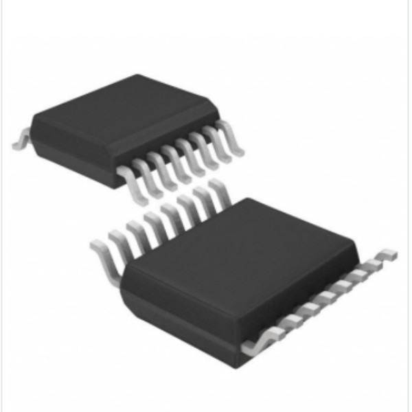
| Package / Case: | TSSOP-16 |
| Core: | S08 |
| Program Memory Size: | 4 kB |
| Data Bus Width: | 8 bit |
| Maximum Clock Frequency: | 40 MHz |
| Data RAM Size: | 256 B |
| Supply Voltage - Min: | 4.5 V |
| Supply Voltage - Max: | 5.5 V |
| Maximum Operating Temperature: | + 85 C |
| Qualification: | AEC-Q100 |
| Packaging: | Tube |
| Brand: | NXP Semiconductors |
| Data RAM Type: | RAM |
| Interface Type: | SCI |
| Moisture Sensitive: | Yes |
| Number of Timers/Counters: | 1 Timer |
| Processor Series: | SC4 |
| Product Type: | 8-bit Microcontrollers - MCU |
| Program Memory Type: | Flash |
| Factory Pack Quantity: | 2880 |
| Subcategory: | Microcontrollers - MCU |
| Part # Aliases: | 935319585574 |
| Unit Weight: | 0.002194 oz |
8-Bit HCS08 Central Processor Unit (CPU)
• Up to 40 MHz HCS08 CPU (central processor unit); up to 20 MHz bus requency
• HC08 instruction set with added BGND instruction
On-Chip Memory
• 4 KB of FLASH with read/program/erase over full operating voltage and emperature
• 256 bytes of Random-access memory (RAM)
Power-Saving Modes
• Two very low power stop modes
• Reduced power wait mode
Clock Source Options
• Oscillator (XOSC) — Loop-control Pierce oscillator; Crystal or ceramic resonator range of 32 kHz to 38.4 kHz or 1 MHz to 16 MHz
• Internal Clock Source (ICS) — Internal clock source module containing a frequency-locked loop (FLL) controlled by internal or external reference; precision trimming of internal reference allows 0.2 % resolution and 2.0 % deviation over temperature and voltage; supports bus frequencies from 2 MHz to 20 MHz.
System Protection
• Watchdog computer operating properly (COP) reset with option to run from dedicated 1 kHz internal clock source or bus clock
• Low-voltage detection with reset or interrupt; selectable trip points
• Illegal opcode detection with reset
• Illegal address detection with reset
• FLASH block protect
• Reset on loss of clock
Development Support
• Single-wire background debug interface
• Breakpoint capability to allow single breakpoint setting during in-circuit debugging
Peripherals
• SCI — Serial Communication Interface
— Full-duplex non-return to zero (NRZ)
— LIN master extended break generation
— LIN slave extended break detection
— Wake-up on active edge
• TPMx — Two 2-channel Timer/PWM modules (TPM1 and TPM2)
— 16-bit modulus or up/down counters
— Input capture, output compare, buffered edge-aligned or center-aligned PWM
• ADC — Analog to Digital Converter
— 8-channel, 10-bit resolution
— 2.5 μs conversion time
— Automatic compare function
— Temperature sensor
— Internal bandgap reference channel
Input/Output
• 12 general purpose I/O pins (GPIOs)
• 8 interrupt pins with selectable polarity
• Hysteresis and configurable pull-up device on all input pins; Configurable slew rate and drive strength on all output pins.
Package Options
• 16-TSSOP
Operating Parameters
• 4.5-5.5 V operation
• C,V, M temperature ranges available, covering -40 – 125 °C operation