AD5697RBRUZ Ethernet ICs Sgl Port Ethernet Phys Layer Xcvr


♠ Product Description
| Product Attribute | Attribute Value |
| Manufacturer: | Analog Devices Inc. |
| Product Category: | Digital to Analog Converters - DAC |
| RoHS: | Details |
| Series: | AD5697R |
| Resolution: | 12 bit |
| Sampling Rate: | - |
| Number of Channels: | 2 Channel |
| Settling Time: | 7 us |
| Output Type: | Voltage Buffered |
| Interface Type: | 2-Wire, I2C |
| Analog Supply Voltage: | 2.7 V to 5.5 V |
| Digital Supply Voltage: | 1.62 V to 5.5 V |
| Minimum Operating Temperature: | - 40 C |
| Maximum Operating Temperature: | + 105 C |
| Mounting Style: | SMD/SMT |
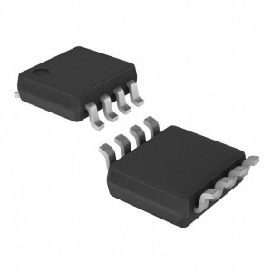
| Package / Case: | TSSOP-16 |
| Packaging: | Tube |
| Brand: | Analog Devices |
| Development Kit: | EVAL-AD5697RSDZ |
| DNL - Differential Nonlinearity: | +/- 1 LSB |
| INL - Integral Nonlinearity: | +/- 1 LSB |
| Product Type: | DACs - Digital to Analog Converters |
| Factory Pack Quantity: | 96 |
| Subcategory: | Data Converter ICs |
| Supply Voltage - Max: | 5.5 V |
| Supply Voltage - Min: | 1.8 V |
| Unit Weight: | 0.006102 oz |
♠ Dual, 12-Bit nanoDAC+ with 2 ppm/°C Reference, I2 C Interface
The AD5697R, a member of the nanoDAC+™ family, is a low power, dual, 12-bit buffered voltage output digital-to-analog converter (DAC). The device includes a 2.5 V, 2 ppm/°C internal reference (enabled by default) and a gain select pin giving a full-scale output of 2.5 V (gain = 1) or 5 V (gain = 2). The AD5697R operates from a single 2.7 V to 5.5 V supply, is guaranteed monotonic by design, and exhibits less than 0.1% FSR gain error and 1.5 mV offset error performance. The device is available in a 3 mm × 3 mm LFCSP and a TSSOP package.
The AD5697R also incorporates a power-on reset circuit and a RSTSEL pin that ensure that the DAC outputs power up to zero scale or midscale and remain there until a valid write takes place. It contains a per channel power-down feature that reduces the current consumption of the device to 4 µA at 3 V while in power-down mode.
The AD5697R uses a versatile 2-wire serial interface that operates at clock rates up to 400 kHz and includes a VLOGIC pin intended for 1.8 V/3 V/5 V logic.
Low drift 2.5 V reference: 2 ppm/°C typical
Tiny package: 3 mm × 3 mm, 16-lead LFCSP
Total unadjusted error (TUE): ±0.1% of full-scale range (FSR) maximum
Offset error: ±1.5 mV maximum
Gain error: ±0.1% of FSR maximum
High drive capability: 20 mA, 0.5 V from supply rails
User selectable gain of 1 or 2 (GAIN pin)
Reset to zero scale or midscale (RSTSEL pin)
1.8 V logic compatibility
Low glitch: 0.5 nV-sec
400 kHz I2C-compatible serial interface
Low power: 3.3 mW at 3 V
2.7 V to 5.5 V power supply
−40°C to +105°C temperature range
Base station power amplifiers
Process controls (programmable logic controller [PLC] I/O cards)
Industrial automation
Data acquisition systems