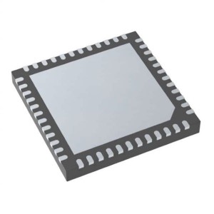
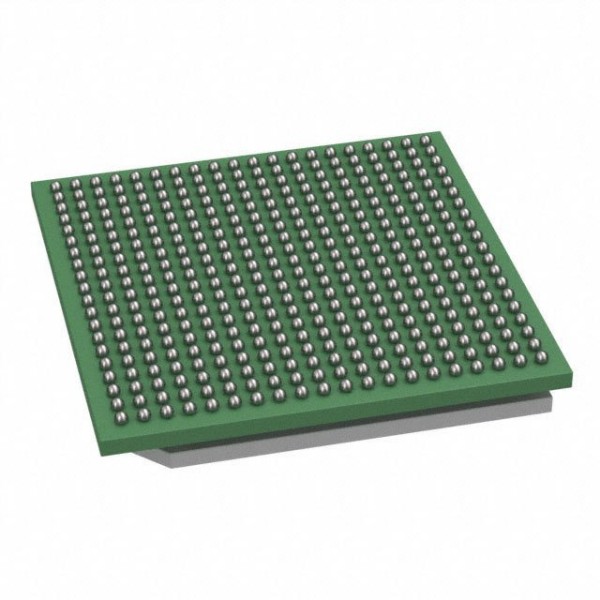
AFE7799IABJ Quad-channel RF transceiver with dual feedback paths 400-FCBGA -40 to 85
♠ Product Description
| Product Attribute | Attribute Value |
| Manufacturer: | Texas Instruments |
| Product Category: | RF Transceiver |
| Type: | Multiband |
| Frequency Range: | 600 MHz to 6 GHz |
| Maximum Data Rate: | 29.5 Gbps |
| Minimum Operating Temperature: | - 40 C |
| Maximum Operating Temperature: | + 85 C |
| Package / Case: | FCBGA-400 |
| Packaging: | Tray |
| Brand: | Texas Instruments |
| Moisture Sensitive: | Yes |
| Mounting Style: | SMD/SMT |
| Number of Receivers: | 4 Receiver |
| Number of Transmitters: | 4 Transmitter |
| Product Type: | RF Transceiver |
| Series: | AFE7799 |
| Factory Pack Quantity: | 90 |
| Subcategory: | Wireless & RF Integrated Circuits |
| Technology: | Si |
♠ AFE7799 Quad-Channel RF Transceiver With Feedback Path
The AFE7799 is a high-performance, multichannel transceiver, integrating four direct up-conversion transmitter chains, four direct down-conversion receiver chains, and two wideband RF sampling digitizing auxiliary chains (feedback paths). The high dynamic range of the transmitter and receiver chains allows generating and receiving 2G, 3G, 4G, and 5G signals for wireless base stations. The low power dissipation and large channels integration makes the AFE7799 suitable to address the power and size constrained 4G and 5G massive MIMO base stations. The wideband and high dynamic range feedback path can assist the digital pre-distortion (DPD) of the power amplifiers in the transmitter chain. The fast SerDes speed can help reducing the number of lanes required to transfer the data in and out.
Each receiver chain of the AFE7799 includes a 28-dB range digital step attenuator (DSA), followed by a wideband passive IQ demodulator, and a baseband amplifier with integrated programmable antialiasing low pass filters, driving a continuous-time sigma-delta ADC. The RX chain can receive an instantaneous bandwidth (IBW) up to 200 MHz. Each receiver channel has two analog peak power detectors and various digital power detectors to assist an external or internal autonomous AGC control for receiver channels, and a RF overload detector for device reliability protection. The integrated QMC (quadrature mismatch compensation) algorithm is capable to continuously monitor and correct for the rx chain I and Q imbalance mismatch without the need to inject any specific signals or perform offline calibration.
Each transmitter chain includes two 14-bit, 3-Gsps IQ DACs, followed by a programmable reconstruction and DAC image rejection filter, an IQ modulator
driving a wideband RF amplifier with 39-dB range gain control. The TX chain integrated QMC and LO leakage cancellation algorithms, leveraging the FB path can constantly track and correct for the TX chain IQ mismatch and LO leakage.
• Quad transmitters based on direct up-conversion architecture:
– Up to 600 MHz of RF transmitted bandwidth per chain
• Quad receivers based on 0-IF down-conversion architecture:
– Up to 200 MHz of RF received bandwidth per chain
• Feedback chain based on RF sampling ADC:
– Up to 600 MHz of RF received bandwidth
• RF frequency range: 600 MHz to 6 GHz
• Wideband fractional-N PLL, VCO for TX and RX LO
• Dedicated integer-N PLL, VCO for data converters clock generation
• JESD204B and JESD204C SerDes interface support:
– 8 SerDes transceivers up to 29.5 Gbps
– 8b/10b and 64b/66b encoding
– 16-bit, 12-bit, 24-bit and 32-bit formatting
– Subclass 1 multi-device synchronization
• Package: 17-mm x 17-mm BGA, 0.8-mm pitch
• Telecom 2G, 3G, 4G, 5G macro, micro base stations
• Telecom 4G, 5G massive MIMO base stations
• Telecom 2G, 3G, 4G, 5G small cell
• Microwave backhaul