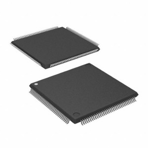
AM3358BZCZA100 Microprocessors – MPU ARM Cortex-A8 MPU

♠ Product Description
| Product Attribute | Attribute Value |
| Manufacturer: | Texas Instruments |
| Product Category: | Microprocessors - MPU |
| RoHS: | Details |
| Mounting Style: | SMD/SMT |
| Package/Case: | PBGA-324 |
| Series: | AM3358 |
| Core: | ARM Cortex A8 |
| Number of Cores: | 1 Core |
| Data Bus Width: | 32 bit |
| Maximum Clock Frequency: | 1 GHz |
| L1 Cache Instruction Memory: | 32 kB |
| L1 Cache Data Memory: | 32 kB |
| Operating Supply Voltage: | 1.325 V |
| Minimum Operating Temperature: | - 40 C |
| Maximum Operating Temperature: | + 105 C |
| Packaging: | Tray |
| Brand: | Texas Instruments |
| Data RAM Size: | 64 kB, 64 kB |
| Data ROM Size: | 176 kB |
| I/O Voltage: | 1.8 V, 3.3 V |
| Interface Type: | CAN, Ethernet, I2C, SPI, UART, USB |
| L2 Cache Instruction / Data Memory: | 256 kB |
| Memory Type: | L1/L2/L3 Cache, RAM, ROM |
| Moisture Sensitive: | Yes |
| Number of Timers/Counters: | 8 Timer |
| Processor Series: | Sitara |
| Product Type: | Microprocessors - MPU |
| Factory Pack Quantity: | 126 |
| Subcategory: | Microprocessors - MPU |
| Tradename: | Sitara |
| Watchdog Timers: | Watchdog Timer |
| Unit Weight: | 1.714 g |
♠ AM335x Sitara™ Processors
The AM335x microprocessors, based on the ARM Cortex-A8 processor, are enhanced with image, graphics processing, peripherals and industrial interface options such as EtherCAT and PROFIBUS. The devices support high-level operating systems (HLOS). Processor SDK Linux® and TI-RTOS are available free of charge from TI.
The AM335x microprocessor contains the subsystems shown in the Functional Block Diagram and a brief description of each follows:
The contains the subsystems shown in the Functional Block Diagram and a brief description of each follows:
The microprocessor unit (MPU) subsystem is based on the ARM Cortex-A8 processor and the PowerVR SGX™ Graphics Accelerator subsystem provides 3D graphics acceleration to support display and gaming effects.
The PRU-ICSS is separate from the ARM core, allowing independent operation and clocking for greater efficiency and flexibility. The PRU-ICSS enables additional peripheral interfaces and real-time protocols such as EtherCAT, PROFINET, EtherNet/IP, PROFIBUS, Ethernet Powerlink, Sercos, and others. Additionally, the programmable nature of the PRU-ICSS, along with its access to pins, events and all system-on-chip (SoC) resources, provides flexibility in implementing fast, real-time responses, specialized data handling operations, custom peripheral interfaces, and in offloading tasks from the other processor cores of SoC.
• Up to 1-GHz Sitara™ ARM® Cortex® -A8 32‑Bit RISC Processor
– NEON™ SIMD Coprocessor
– 32KB of L1 Instruction and 32KB of Data Cache With Single-Error Detection (Parity)
– 256KB of L2 Cache With Error Correcting Code (ECC)
– 176KB of On-Chip Boot ROM
– 64KB of Dedicated RAM
– Emulation and Debug – JTAG
– Interrupt Controller (up to 128 Interrupt Requests)
• On-Chip Memory (Shared L3 RAM)
– 64KB of General-Purpose On-Chip Memory Controller (OCMC) RAM
– Accessible to All Masters
– Supports Retention for Fast Wakeup
• External Memory Interfaces (EMIF)
– mDDR(LPDDR), DDR2, DDR3, DDR3L Controller:
– mDDR: 200-MHz Clock (400-MHz Data Rate)
– DDR2: 266-MHz Clock (532-MHz Data Rate)
– DDR3: 400-MHz Clock (800-MHz Data Rate)
– DDR3L: 400-MHz Clock (800-MHz Data Rate)
– 16-Bit Data Bus – 1GB of Total Addressable Space
– Supports One x16 or Two x8 Memory Device Configurations
– General-Purpose Memory Controller (GPMC)
– Flexible 8-Bit and 16-Bit Asynchronous Memory Interface With up to Seven Chip Selects (NAND, NOR, Muxed-NOR, SRAM)
– Uses BCH Code to Support 4-, 8-, or 16-Bit ECC
– Uses Hamming Code to Support 1-Bit ECC
– Error Locator Module (ELM)
– Used in Conjunction With the GPMC to Locate Addresses of Data Errors from Syndrome Polynomials Generated Using a BCH Algorithm
– Supports 4-, 8-, and 16-Bit per 512-Byte Block Error Location Based on BCH Algorithms
• Programmable Real-Time Unit Subsystem and Industrial Communication Subsystem (PRU-ICSS)
– Supports Protocols such as EtherCAT® ,PROFIBUS, PROFINET, EtherNet/IP™, and More
– Two Programmable Real-Time Units (PRUs)
– 32-Bit Load/Store RISC Processor Capable of Running at 200 MHz
– 8KB of Instruction RAM With Single-Error Detection (Parity)
– 8KB of Data RAM With Single-Error Detection (Parity)
– Single-Cycle 32-Bit Multiplier With 64-Bit Accumulator
– Enhanced GPIO Module Provides Shift-In/Out Support and Parallel Latch on External Signal
– 12KB of Shared RAM With Single-Error Detection (Parity)
– Three 120-Byte Register Banks Accessible by Each PRU
– Interrupt Controller (INTC) for Handling System Input Events
– Local Interconnect Bus for Connecting Internal and External Masters to the Resources Inside the PRU-ICSS
– Peripherals Inside the PRU-ICSS:
– One UART Port With Flow Control Pins, Supports up to 12 Mbps
– One Enhanced Capture (eCAP) Module
– Two MII Ethernet Ports that Support Industrial Ethernet, such as EtherCAT
– One MDIO Port
• Power, Reset, and Clock Management (PRCM) Module
– Controls the Entry and Exit of Stand-By and Deep-Sleep Modes
– Responsible for Sleep Sequencing, Power Domain Switch-Off Sequencing, Wake-Up Sequencing, and Power Domain Switch-On Sequencing
– Clocks
– Integrated 15- to 35-MHz High-Frequency Oscillator Used to Generate a Reference Clock for Various System and Peripheral Clocks
– Supports Individual Clock Enable and Disable Control for Subsystems and Peripherals to Facilitate Reduced Power Consumption
– Five ADPLLs to Generate System Clocks (MPU Subsystem, DDR Interface, USB andPeripherals [MMC and SD, UART, SPI, I 2C], L3, L4, Ethernet, GFX [SGX530], LCD Pixel Clock)
– Power
– Two Nonswitchable Power Domains (Real-Time Clock [RTC], Wake-Up Logic [WAKEUP])
– Three Switchable Power Domains (MPU Subsystem [MPU], SGX530 [GFX], Peripherals and Infrastructure [PER])
– Implements SmartReflex™ Class 2B for Core Voltage Scaling Based On Die Temperature, Process Variation, and Performance (Adaptive Voltage Scaling [AVS])
– Dynamic Voltage Frequency Scaling (DVFS)
• Gaming Peripherals
• Home and Industrial Automation
• Consumer Medical Appliances
• Printers
• Smart Toll Systems
• Connected Vending Machines
• Weighing Scales
• Educational Consoles
• Advanced Toys