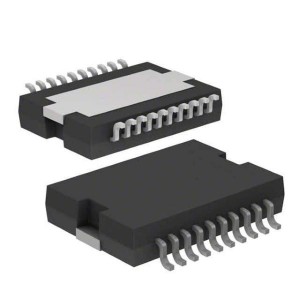
CD74HC123PWR Monostable Multi-vibrator Dual Retrig Mono

♠ Product Description
|
Product Attribute |
Attribute Value |
|
Manufacturer: |
Texas Instruments |
|
Product Category: |
Monostable Multi-vibrator |
|
RoHS: |
Details |
|
Elements per Chip: |
2 |
|
Logic Family: |
HC |
|
Logic Type: |
Monostable Multivibrator |
|
Package/Case: |
TSSOP-16 |
|
Supply Current - Max: |
0.008 mA |
|
Propagation Delay Time: |
320 ns, 64 ns, 54 ns |
|
High Level Output Current: |
- 5.2 mA |
|
Low Level Output Current: |
5.2 mA |
|
Supply Voltage - Max: |
6 V |
|
Supply Voltage - Min: |
2 V |
|
Minimum Operating Temperature: |
- 55 C |
|
Maximum Operating Temperature: |
+ 125 C |
|
Packaging: |
Reel |
|
Packaging: |
Cut Tape |
|
Packaging: |
MouseReel |
|
Brand: |
Texas Instruments |
|
Height: |
1.15 mm |
|
Length: |
5 mm |
|
Mounting Style: |
SMD/SMT |
|
Operating Supply Voltage: |
2.5 V, 3.3 V, 5 V |
|
Product Type: |
Monostable Multivibrator |
|
Series: |
CD74HC123 |
|
Factory Pack Quantity: |
2000 |
|
Subcategory: |
Logic ICs |
|
Width: |
4.4 mm |
|
Unit Weight: |
62 mg |
♠ High-Speed CMOS Logic Dual Retriggerable Monostable Multivibrators with Resets
The ’HC123, ’HCT123, CD74HC423 and CD74HCT423 are dual monostable multivibrators with resets. They are all retriggerable and differ only in that the 123 types can be triggered by a negative to positive reset pulse; whereas the 423 types do not have this feature. An external resistor (RX) and an external capacitor (CX) control the timing and the accuracy for the circuit. Adjustment of Rx and CX provides a wide range of output pulse widths from the Q and Q terminals. Pulse triggering on the A and B inputs occur at a particular voltage level and is not related to the rise and fall times of the trigger pulses.
Once triggered, the output pulse width may be extended by retriggering inputs A and B. The output pulse can be terminated by a LOW level on the Reset (R) pin. Trailing edge triggering (A) and leading edge triggering (B) inputs are provided for triggering from either edge of the input pulse. If either Mono is not used each input on the unused device (A, B, and R) must be terminated high or low. The minimum value of external resistance, Rx is typically 5kΩ. The minimum value external capacitance, CX, is 0pF. The calculation for the pulse width is tW = 0.45 RXCX at VCC = 5V
• Overriding Reset Terminates Output Pulse
• Triggering From the Leading or Trailing Edge
• Q and Q Buffered Outputs
• Separate Resets
• Wide Range of Output-Pulse Widths
• Schmitt Trigger on Both A and B Inputs
• Fanout (Over Temperature Range)
– Standard Outputs . . . . . . . . . . . . . . . 10 LSTTL Loads
– Bus Driver Outputs . . . . . . . . . . . . . 15 LSTTL Loads
• Wide Operating Temperature Range . . . -55oC to 125oC
• Balanced Propagation Delay and Transition Times
• Significant Power Reduction Compared to LSTTL Logic ICs
• HC Types
– 2V to 6V Operation
– High Noise Immunity: NIL = 30%, NIH = 30%of VCC at VCC = 5V
• HCT Types
– 4.5V to 5.5V Operation
– Direct LSTTL Input Logic Compatibility, VIL= 0.8V (Max), VIH = 2V (Min) – CMOS Input Compatibility, Il ≤ 1µA at VOL, VOH