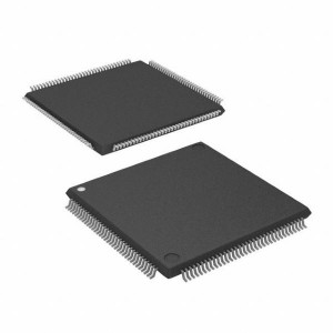
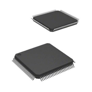
LCMXO2-2000HC-4BG256C FPGA – Field Programmable Gate Array 2112 LUTs 207 IO 3.3V 4 Spd

♠ Product Description
| Product Attribute | Attribute Value |
| Manufacturer: | Lattice |
| Product Category: | FPGA - Field Programmable Gate Array |
| RoHS: | Details |
| Series: | LCMXO2 |
| Number of Logic Elements: | 2112 LE |
| Number of I/Os: | 206 I/O |
| Supply Voltage - Min: | 2.375 V |
| Supply Voltage - Max: | 3.6 V |
| Minimum Operating Temperature: | 0 C |
| Maximum Operating Temperature: | + 85 C |
| Data Rate: | - |
| Number of Transceivers: | - |
| Mounting Style: | SMD/SMT |
| Package / Case: | CABGA-256 |
| Packaging: | Tray |
| Brand: | Lattice |
| Distributed RAM: | 16 kbit |
| Embedded Block RAM - EBR: | 74 kbit |
| Maximum Operating Frequency: | 269 MHz |
| Moisture Sensitive: | Yes |
| Number of Logic Array Blocks - LABs: | 264 LAB |
| Operating Supply Current: | 4.8 mA |
| Operating Supply Voltage: | 2.5 V/3.3 V |
| Product Type: | FPGA - Field Programmable Gate Array |
| Factory Pack Quantity: | 119 |
| Subcategory: | Programmable Logic ICs |
| Total Memory: | 170 kbit |
| Tradename: | MachXO2 |
| Unit Weight: | 0.429319 oz |
1. Flexible Logic Architecture
• Six devices with 256 to 6864 LUT4s and 18 to 334 I/Os Ultra Low Power Devices
• Advanced 65 nm low power process
• As low as 22 µW standby power
• Programmable low swing differential I/Os
• Stand-by mode and other power saving options 2. Embedded and Distributed Memory
• Up to 240 kbits sysMEM™ Embedded Block RAM
• Up to 54 kbits Distributed RAM
• Dedicated FIFO control logic
3. On-Chip User Flash Memory
• Up to 256 kbits of User Flash Memory
• 100,000 write cycles
• Accessible through WISHBONE, SPI, I2 C and JTAG interfaces
• Can be used as soft processor PROM or as Flash memory
4. Pre-Engineered Source Synchronous I/O
• DDR registers in I/O cells
• Dedicated gearing logic
• 7:1 Gearing for Display I/Os
• Generic DDR, DDRX2, DDRX4
• Dedicated DDR/DDR2/LPDDR memory with DQS support
5. High Performance, Flexible I/O Buffer
• Programmable sysIO™ buffer supports wide range of interfaces:
– LVCMOS 3.3/2.5/1.8/1.5/1.2
– LVTTL
– PCI
– LVDS, Bus-LVDS, MLVDS, RSDS, LVPECL
– SSTL 25/18
– HSTL 18
– Schmitt trigger inputs, up to 0.5 V hysteresis
• I/Os support hot socketing
• On-chip differential termination
• Programmable pull-up or pull-down mode
6. Flexible On-Chip Clocking
• Eight primary clocks
• Up to two edge clocks for high-speed I/O interfaces (top and bottom sides only)
• Up to two analog PLLs per device with fractional-n frequency synthesis
– Wide input frequency range (7 MHz to 400 MHz)
7. Non-volatile, Infinitely Reconfigurable
• Instant-on
– powers up in microseconds
• Single-chip, secure solution
• Programmable through JTAG, SPI or I2 C
• Supports background programming of non-vola
8.tile memory
• Optional dual boot with external SPI memory
9. TransFR™ Reconfiguration
• In-field logic update while system operates
10. Enhanced System Level Support
• On-chip hardened functions: SPI, I2 C, timer/ counter
• On-chip oscillator with 5.5% accuracy
• Unique TraceID for system tracking
• One Time Programmable (OTP) mode
• Single power supply with extended operating range
• IEEE Standard 1149.1 boundary scan
• IEEE 1532 compliant in-system programming
11. Broad Range of Package Options
• TQFP, WLCSP, ucBGA, csBGA, caBGA, ftBGA, fpBGA, QFN package options
• Small footprint package options
– As small as 2.5 mm x 2.5 mm
• Density migration supported
• Advanced halogen-free packaging