SN65DSI84TPAPRQ1 Auto Sngl Ch MIPI DSI to SnglLink LVDS
♠ Product Description
| Product Attribute | Attribute Value |
| Manufacturer: | Texas Instruments |
| Product Category: | LVDS Interface IC |
| Type: | DSI to Dual-Link LVDS Bridge |
| Number of Drivers: | 8 Driver |
| Number of Receivers: | 4 Receiver |
| Data Rate: | 1.078 Gb/s |
| Input Type: | MIPI D-PHY |
| Output Type: | LVDS |
| Supply Voltage - Max: | 1.95 V |
| Supply Voltage - Min: | 1.65 V |
| Minimum Operating Temperature: | - 40 C |
| Maximum Operating Temperature: | + 105 C |
| Mounting Style: | SMD/SMT |
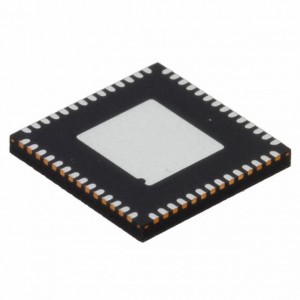
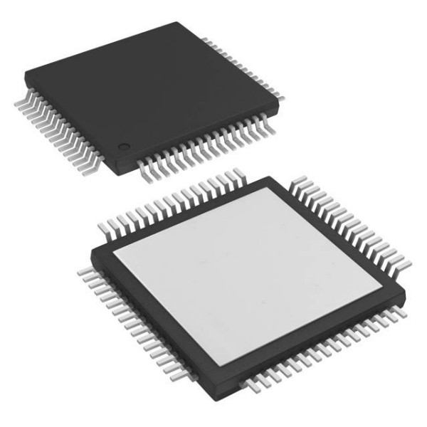
| Package / Case: | HTQFP-64 |
| Qualification: | AEC-Q100 |
| Packaging: | Reel |
| Packaging: | Cut Tape |
| Packaging: | MouseReel |
| Brand: | Texas Instruments |
| Moisture Sensitive: | Yes |
| Operating Supply Current: | 106 mA |
| Product Type: | LVDS Interface IC |
| Series: | SN65DSI84-Q1 |
| Factory Pack Quantity: | 1000 |
| Subcategory: | Interface ICs |
| Unit Weight: | 0.010780 oz |
♠ SN65DSI84-Q1 Automotive Single-Channel MIPI® DSI to Dual-Link LVDS Bridge
The SN65DSI84-Q1 DSI-to-LVDS bridge features a single-channel MIPI D-PHY receiver front-end configuration with four lanes per channel operating at 1 Gbps per lane and a maximum input bandwidth of 4 Gbps. The bridge decodes MIPI® DSI 18-bpp RGB666 and 24-bpp RGB888 packets and converts the formatted video data-stream to an LVDS output operating at pixel clocks operating from 25 MHz to 154 MHz, offering a dual-link LVDS or single-link LVDS with four data lanes per link.
The SN65DSI84-Q1 device is well suited for WUXGA (1920 × 1080) at 60 frames per second (fps) with up to 24 bits-per-pixel (bpp). Partial line buffering is implemented to accommodate the data stream mismatch between the DSI and LVDS interfaces.
The SN65DSI84-Q1 device is implemented in a small outline 10 mm × 10 mm HTQFP package with a 0.5-mm pitch, and operates across a temperature range from –40°C to 105°C.
1• Qualified for Automotive Applications
• AEC-Q100 Qualified With the Following Results:
– Device Temperature Grade 2: –40°C to 105°C Ambient Operating Temperature
– Device HBM ESD Classification Level 3A
– Device CDM ESD Classification Level C6
• Implements MIPI D-PHY Version 1.00.00 Physical Layer Front-End and Display Serial Interface (DSI) Version 1.02.00
• Single-Channel DSI Receiver Configurable for One, Two, Three, or Four D-PHY Data Lanes Per Channel Operating up to 1 Gbps Per Lane
• Supports 18-bpp and 24-bpp DSI Video Packets with RGB666 and RGB888 Formats
• Suitable for 60-fps WUXGA 1920 × 1200 Resolution at 18-bpp and 24-bpp Color, and 60- fps 1366 × 768 Resolution at 18-bpp and 24-bpp
• Output Configurable for Single-Link or Dual-Link LVDS
• Supports Single-Channel DSI to Dual-Link LVDS Operating Mode
• LVDS Output-Clock Range of 25 MHz to 154 MHz in Dual-Link or Single-Link Mode
• LVDS Pixel Clock May be Sourced from FreeRunning Continuous D-PHY Clock or External Reference Clock (REFCLK)
• 1.8 V Main VCC Power Supply
• Low Power Features Include SHUTDOWN Mode, Reduced LVDS Output Voltage Swing, Common Mode, and MIPI Ultra-Low Power State (ULPS) Support
• LVDS Channel SWAP, LVDS PIN Order Reverse Feature for Ease of PCB Routing
• Packaged in 64-pin 10 mm × 10 mm HTQFP (PAP) PowerPAD™ IC Package
• Infotainment Head Unit With Integrated Display
• Infotainment Head Unit With Remote Display
• Infotainment Rear-Seat Entertainment
• Hybrid Automotive Cluster
• Portable Navigation Device (PND)
• Navigation
• Industrial Human Machine Interface (HMI) and Displays