TPS61170QDRVRQ1 AC 1.2A SWITCH,HIGH VLTG BOOST CONVERTER
♠ Product Description
| Product Attribute | Attribute Value |
| Manufacturer: | Texas Instruments |
| Product Category: | Switching Voltage Regulators |
| Mounting Style: | SMD/SMT |
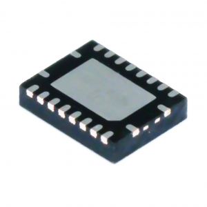
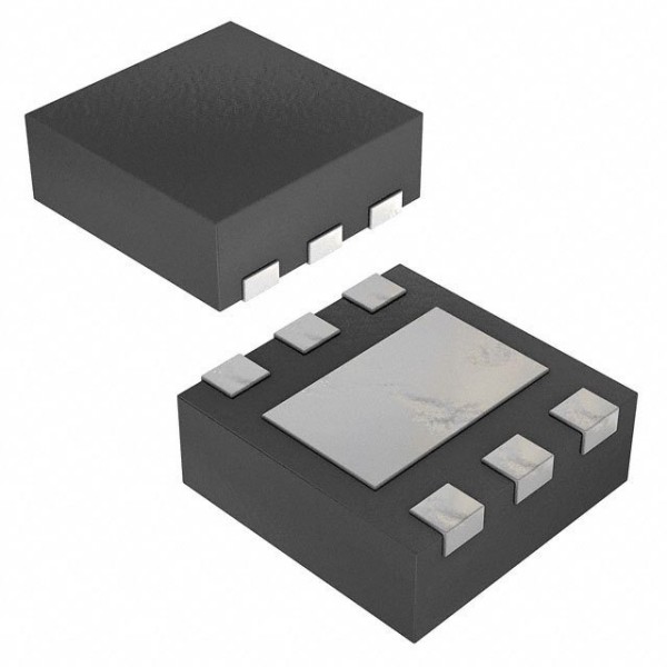
| Package / Case: | WSON-6 |
| Topology: | Boost |
| Output Voltage: | 3 V to 38 V |
| Output Current: | 1.2 A |
| Number of Outputs: | 1 Output |
| Input Voltage, Min: | 3 V |
| Input Voltage, Max: | 18 V |
| Quiescent Current: | 2.3 mA |
| Switching Frequency: | 1.2 MHz |
| Minimum Operating Temperature: | - 40 C |
| Maximum Operating Temperature: | + 125 C |
| Qualification: | AEC-Q100 |
| Series: | TPS61170-Q1 |
| Packaging: | Reel |
| Packaging: | Cut Tape |
| Packaging: | MouseReel |
| Brand: | Texas Instruments |
| Input Voltage: | 3 V to 18 V |
| Moisture Sensitive: | Yes |
| Operating Supply Current: | 2.3 mA |
| Product: | Voltage Regulators |
| Product Type: | Switching Voltage Regulators |
| Factory Pack Quantity: | 3000 |
| Subcategory: | PMIC - Power Management ICs |
| Type: | Voltage Converter |
| Unit Weight: | 0.000342 oz |
♠ TPS61170-Q1 1.2-A High-Voltage Boost Converter in 2-mm × 2-mm SON Package
The TPS61170-Q1 is a monolithic, high-voltage switching regulator with integrated 1.2-A, 40-V power MOSFET. The device can be configured in several standard switching-regulator topologies, including boost and SEPIC. The device has a wide inputvoltage range to support applications with input voltage from multicell batteries or regulated 5-V, 12-V power rails.
The TPS61170-Q1 operates at a 1.2-MHz switching frequency, allowing the use of low-profile inductors and low-value ceramic input and output capacitors. External loop compensation components give the user flexibility to optimize loop compensation and transient response. The device has built-in protection features, such as pulse-by-pulse overcurrent limit, soft start, and thermal shutdown.
The FB pin regulates to a reference voltage of 1.229 V. The reference voltage can be lowered using a 1-wire digital interface (EasyScale™ protocol) through the CTRL pin. Alternatively, a pulse widthmodulation (PWM) signal can be applied to the CTRL pin. The duty cycle of the signal reduces the feedback reference voltage proportionally.
The TPS61170-Q1 is available in a 6-pin 2-mm × 2-mm SON package, allowing a compact powersupply solution.
• Qualified for automotive applications
• Functional Safety-Capable
– Documentation available to aid functional safety system design
• 3-V to 18-V Input voltage range
• High output voltage: up to 38 V
• 1.2-A Integrated switch
• 1.2-MHz Fixed switching frequency
• 12 V at 300 mA and 24 V at 150 mA from 5-V Input (typical)
• Up to 93% efficiency
• On-the-fly output voltage reprogramming
• Skip-switching cycle for output regulation at light load
• Built-in soft start
• 6-Pin, 2-mm × 2-mm SON package
• HEV and EV charger systems
• Advanced driver assistance systems (ADAS)