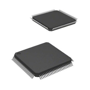
SPC5634MF2MLQ80 32-bit Microcontrollers – MCU NXP 32-bit MCU, Power Arch core, 1.5MB Flash, 80MHz, -40/+125degC, Automotive Grade, QFP 144
♠ Product Description
| Product Attribute | Attribute Value |
| Manufacturer: | NXP |
| Product Category: | 32-bit Microcontrollers - MCU |
| RoHS: | Details |
| Series: | MPC5634M |
| Mounting Style: | SMD/SMT |
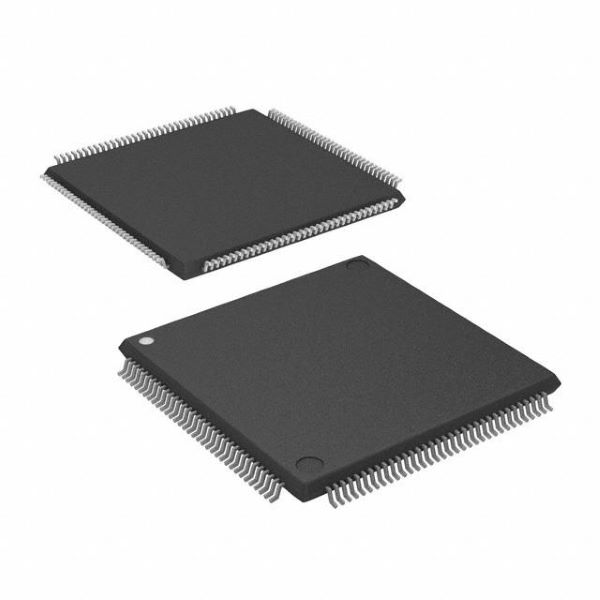
| Package/Case: | LQFP-144 |
| Core: | e200z3 |
| Program Memory Size: | 1.5 MB |
| Data RAM Size: | 94 kB |
| Data Bus Width: | 32 bit |
| ADC Resolution: | 2 x 8 bit/10 bit/12 bit |
| Maximum Clock Frequency: | 80 MHz |
| Number of I/Os: | 80 I/O |
| Supply Voltage - Min: | 1.14 V |
| Supply Voltage - Max: | 1.32 V |
| Minimum Operating Temperature: | - 40 C |
| Maximum Operating Temperature: | + 150 C |
| Qualification: | AEC-Q100 |
| Packaging: | Tray |
| Analogue Supply Voltage: | 5.25 V |
| Brand: | NXP Semiconductors |
| Data RAM Type: | SRAM |
| I/O Voltage: | 5.25 V |
| Moisture Sensitive: | Yes |
| Product: | MCU |
| Product Type: | 32-bit Microcontrollers - MCU |
| Program Memory Type: | Flash |
| Factory Pack Quantity: | 60 |
| Subcategory: | Microcontrollers - MCU |
| Watchdog Timers: | Watchdog Timer |
| Part # Aliases: | 935311091557 |
| Unit Weight: | 1.319 g |
♠ 32-bit Microcontrollers - MCU
These 32-bit automotive microcontrollers are a family of system-on-chip (SoC) devices that contain all the features of the MPC5500 family and many new features coupled with high performance 90 nm CMOS technology to provide substantial reduction of cost per feature and significant performance improvement. The advanced and cost-efficient host processor core of this automotive controller family is built on Power Architecture® technology. This family contains enhancements that improve the architecture’s fit in embedded applications, includes additional instruction support for digital signal processing (DSP), integrates technologies—such as an enhanced time processor unit, enhanced queued analog-to-digital converter, Controller Area Network, and an enhanced modular input-output system—that are important for today’s lower-end powertrain applications. This device family is a completely compatible extension to Freescale’s MPC5500 family. The device has a single level of memory hierarchy consisting of up to 94 KB on-chip SRAM and up to 1.5 MB of internal flash memory. The device also has an external bus interface (EBI) for ‘calibration’. This external bus interface has been designed to support most of the standard memories used with the MPC5xx and MPC55xx families.
• Operating Parameters
— Fully static operation, 0 MHz– 80 MHz (plus 2% frequency modulation – 82 MHz)
— –40 ℃ to 150 ℃ junction temperature operating range
— Low power design
– Less than 400 mW power dissipation (nominal)
– Designed for dynamic power management of core and peripherals
– Software controlled clock gating of peripherals
– Low power stop mode, with all clocks stopped
— Fabricated in 90 nm process
— 1.2 V internal logic
— Single power supply with 5.0 V -10%/+5% (4.5 V to 5.25 V) with internal regulator to provide 3.3 V and 1.2 V for the core
— Input and output pins with 5.0 V -10%/+5% (4.5 V to 5.25 V) range
– 35%/65% VDDE CMOS switch levels (with hysteresis)
– Selectable hysteresis
– Selectable slew rate control
— Nexus pins powered by 3.3 V supply
— Designed with EMI reduction techniques
– Phase-locked loop
– Frequency modulation of system clock frequency
– On-chip bypass capacitance
– Selectable slew rate and drive strength
• High performance e200z335 core processor
— 32-bit Power Architecture Book E programmer’s model
— Variable Length Encoding Enhancements
– Allows Power Architecture instruction set to be optionally encoded in a mixed 16 and 32-bit instructions
– Results in smaller code size
— Single issue, 32-bit Power Architecture technology compliant CPU
— In-order execution and retirement
— Precise exception handling
— Branch processing unit
– Dedicated branch address calculation adder
– Branch acceleration using Branch Lookahead Instruction Buffer
— Load/store unit
– One-cycle load latency
– Fully pipelined
– Big and Little Endian support
– Misaligned access support
– Zero load-to-use pipeline bubbles
— Thirty-two 64-bit general purpose registers (GPRs)
— Memory management unit (MMU) with 16-entry fully-associative translation look-aside buffer (TLB)
— Separate instruction bus and load/store bus
— Vectored interrupt support
— Interrupt latency < 120 ns @ 80 MHz (measured from interrupt request to execution of first instruction of interrupt exception handler)