TPS51604DSGR Gate Drivers Sync Buck FET Dvr

♠ Product Description
| Product Attribute | Attribute Value |
| Manufacturer: | Texas Instruments |
| Product Category: | Gate Drivers |
| RoHS: | Details |
| Product: | Half-Bridge Drivers |
| Type: | High-Side, Low-Side |
| Mounting Style: | SMD/SMT |
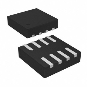
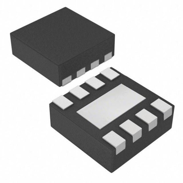
| Package / Case: | WSON-8 |
| Number of Drivers: | 2 Driver |
| Number of Outputs: | 2 Output |
| Output Current: | 4 A |
| Supply Voltage - Min: | 4.5 V |
| Supply Voltage - Max: | 5.5 V |
| Rise Time: | 15 ns |
| Fall Time: | 10 ns |
| Minimum Operating Temperature: | - 40 C |
| Maximum Operating Temperature: | + 105 C |
| Series: | TPS51604 |
| Packaging: | Reel |
| Packaging: | Cut Tape |
| Packaging: | MouseReel |
| Brand: | Texas Instruments |
| Features: | Dead Time Control, Synchronous Rectification |
| Moisture Sensitive: | Yes |
| Operating Supply Current: | 600 uA |
| Operating Supply Voltage: | 4.5 V to 28 V |
| Output Voltage: | 34 V |
| Product Type: | Gate Drivers |
| Factory Pack Quantity: | 3000 |
| Subcategory: | PMIC - Power Management ICs |
| Technology: | Si |
| Unit Weight: | 0.000384 oz |
♠ TPS51604 Synchronous Buck FET Driver for High-Frequency CPU Core Power
The TPS51604 drivers are optimized for high frequency CPU VCORE applications. Advanced features such as reduced dead-time drive and auto zero crossing are used to optimize efficiency over the entire load range.
The SKIP pin provides the option of CCM operation to support controlled management of the output voltage. In addition, the TPS51604 supports two low power modes. With the PWM input in tri-state, quiescent current is reduced to 130 µA, with immediate response. When SKIP is held at tri-state, the current is reduced to 8 µA (typically 20 µs is required to resume switching). Paired with the appropriate TI controller, the drivers deliver an exceptionally high performance power supply system.
The TPS51604 device is packaged in a space saving, thermally-enhanced 8-pin, 2-mm x 2-mm WSON package and operates from –40°C to 105°C.
• Reduced Dead-Time Drive Circuit for Optimized CCM
• Automatic Zero Crossing Detection for Optimized DCM Efficiency
• Multiple Low-Power Modes for Optimized Light- Load Efficiency
• Optimized Signal Path Delays for High-Frequency Operation
• Integrated BST Switch Drive Strength Optimized for Ultrabook FETs
• Optimized for 5-V FET Drive
• Conversion Input Voltage Range (VIN): 4.5 to 28 V
• 2-mm × 2-mm, 8-Pin, WSON Thermal Pad Package
• Tablets Using High-Frequency CPUs With the Following Power Input:
– Adapter
– Battery
– NVDC
– 5-V or 12-V Rails