TPS61240IDRVRQ1 5V,400mA,4MHz Step- Up DC/DC Converter
♠ Product Description
| Product Attribute | Attribute Value |
| Manufacturer: | Texas Instruments |
| Product Category: | Switching Voltage Regulators |
| Mounting Style: | SMD/SMT |
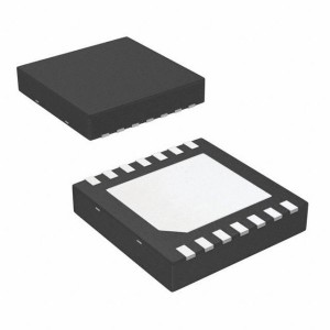
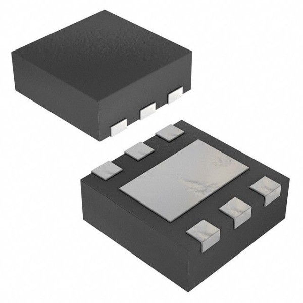
| Package / Case: | WSON-6 |
| Topology: | Boost |
| Output Voltage: | 5 V |
| Output Current: | 600 mA |
| Number of Outputs: | 1 Output |
| Input Voltage, Min: | 2.3 V |
| Input Voltage, Max: | 5.5 V |
| Quiescent Current: | 30 uA |
| Switching Frequency: | 3.5 MHz |
| Minimum Operating Temperature: | - 40 C |
| Maximum Operating Temperature: | + 105 C |
| Qualification: | AEC-Q100 |
| Series: | TPS61240-Q1 |
| Packaging: | Reel |
| Packaging: | Cut Tape |
| Packaging: | MouseReel |
| Brand: | Texas Instruments |
| Input Voltage: | 2.3 V to 5.5 V |
| Moisture Sensitive: | Yes |
| Operating Supply Current: | 30 uA |
| Product: | Voltage Regulators |
| Product Type: | Switching Voltage Regulators |
| Factory Pack Quantity: | 3000 |
| Subcategory: | PMIC - Power Management ICs |
| Type: | Voltage Converter |
| Unit Weight: | 0.000342 oz |
♠ TPS61240-Q1 3.5-MHz High Efficiency Step-Up Converter
The TPS61240-Q1 device is a high efficient synchronous step up DC-DC converter optimized for products powered by either a three-cell alkaline, NiCd or NiMH, or one-cell Li-Ion or Li-Polymer battery. The TPS61240-Q1 supports output currents up to 450 mA. The TPS61240-Q1 has an input valley current
limit of 500 mA.
TPS61240-Q1 device provides fixed output voltage of 5V-typ with an input voltage range of 2.3 V to 5.5 V and the device supports batteries with extended voltage range. During shutdown, the load is completely disconnected from the battery. The TPS61240-Q1 boost converter is based on a quasiconstant on-time valley current mode control scheme.
The TPS61240-Q1 presents a high impedance at the VOUT pin when shut down. This allows for use in applications that require the regulated output bus to be driven by another supply while the TPS61240-Q1 is shut down.
During light loads the device will automatically pulse skip allowing maximum efficiency at lowest quiescent currents. In the shutdown mode, the current consumption is reduced to less than 1 μA.
TPS61240-Q1 allows the use of a small inductor and capacitors to achieve a small solution size. The TPS61240-Q1 is available in a 2 mm × 2 mm WSON package
• Qualified for automotive applications
• AEC-Q100 qualified with the following results:
– Device temperature grade
– TPS61240IDRVRQ1: grade 3, –40°C to +85°C ambient operating temperature
– TPS61240TDRVRQ1: grade 2, –40°C to +105°C ambient operating temperature
– Device HBM ESD classification level 2
– Device CDM ESD classification level C6
• Functional Safety-Capable
– Documentation available to aid functional safety system design
• Efficiency > 90% at nominal operating conditions
• Total DC Output Voltage Accuracy 5 V ±2%
• Typical 30-μA quiescent current
• Best in class line and load transient
• Wide VIN range from 2.3 V to 5.5 V
• Output current up to 450 mA
• Automatic PFM/PWM mode transition
• Low ripple power save mode for improved efficiency at light loads
• Internal soft start, 250 μs typical start-up time
• 3.5-MHz typical operating frequency
• Load disconnect during shutdown
• Current overload and thermal shutdown protection
• Only three surface-mount external components required (one MLCC inductor, two ceramic capacitors)
• Total solution size < 13 mm2
• Available in a 2 mm × 2 mm WSON package
• Advanced driver assistance systems (ADAS)
– Front camera
– Surround view system ECU
– Radar and LIDAR
• Automotive infotainment and cluster
– Head unit
– HMI and display
• Body electronics and lighting
• Factory automation and contro