ATXMEGA128A1U-AU 8bit Microcontrollers MCU 100TQFP IND TEMP GREEN 1.6-3.6V

♠ Product Description
| Product Attribute | Attribute Value |
| Manufacturer: | Microchip |
| Product Category: | 8-bit Microcontrollers - MCU |
| RoHS: | Details |
| Series: | XMEGA A1U |
| Mounting Style: | SMD/SMT |
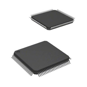
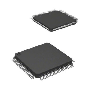
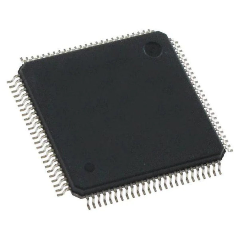
| Package / Case: | TQFP-100 |
| Core: | AVR |
| Program Memory Size: | 128 kB |
| Data Bus Width: | 8 bit/16 bit |
| ADC Resolution: | 12 bit |
| Maximum Clock Frequency: | 32 MHz |
| Number of I/Os: | 78 I/O |
| Data RAM Size: | 8 kB |
| Supply Voltage - Min: | 1.6 V |
| Supply Voltage - Max: | 3.6 V |
| Minimum Operating Temperature: | - 40 C |
| Maximum Operating Temperature: | + 105 C |
| Packaging: | Tray |
| Brand: | Microchip Technology / Atmel |
| Data RAM Type: | SRAM |
| Data ROM Size: | 2 kB |
| Data ROM Type: | EEPROM |
| Interface Type: | I2C, SPI, UART |
| Moisture Sensitive: | Yes |
| Number of ADC Channels: | 16 Channel |
| Number of Timers/Counters: | 8 Timer |
| Processor Series: | AVR XMEGA |
| Product: | MCU |
| Product Type: | 8-bit Microcontrollers - MCU |
| Program Memory Type: | Flash |
| Factory Pack Quantity: | 90 |
| Subcategory: | Microcontrollers - MCU |
| Tradename: | XMEGA |
| Unit Weight: | 0.023175 oz |
♠ 8/16-bit Atmel XMEGA A1U Microcontroller
The Atmel AVR XMEGA is a family of low power, high performance, and peripheral rich 8/16-bit microcontrollers based on the AVR enhanced RISC architecture. By executing instructions in a single clock cycle, the AVR XMEGA devices achieve CPU throughput approaching one million instructions per second (MIPS) per megahertz, allowing the system designer to optimize power consumption versus processing speed.
The Atmel AVR CPU combines a rich instruction set with 32 general purpose working registers. All 32 registers are directly connected to the arithmetic logic unit (ALU), allowing two independent registers to be accessed in a single instruction, executed in one clock cycle. The resulting architecture is more code efficient while achieving throughputs many times faster than conventional single-accumulator or CISC based microcontrollers.
The AVR XMEGA A1U devices provide the following features: in-system programmable flash with read-while-write capabilities; internal EEPROM and SRAM; four-channel DMA controller, eight-channel event system and programmable multilevel interrupt controller, 78 general purpose I/O lines, 16-bit real-time counter (RTC); eight flexible, 16-bit timer/counters with compare and PWM channels, eight USARTs; four two-wire serial interfaces (TWIs); one full speed USB 2.0 interface; four serial peripheral interfaces (SPIs); AES and DES cryptographic engine; CRC-16 (CRC-CCITT) and CRC-32 (IEEE 802.3) generator; two 16-channel, 12-bit ADCs with programmable gain; two 2-channel, 12-bit DACs; four Analog Comparators (ACs) with window mode; programmable watchdog timer with separate internal oscillator; accurate internal oscillators with PLL and prescaler; and programmable brown-out detection.
The program and debug interface (PDI), a fast, two-pin interface for programming and debugging, is available. The devices also have an IEEE std. 1149.1 compliant JTAG interface, and this can also be used for boundary scan, on-chip debug and programming.
The XMEGA A1U devices have five software selectable power saving modes. The idle mode stops the CPU while allowing the SRAM, DMA controller, event system, interrupt controller, and all peripherals to continue functioning. The power-down mode saves the SRAM and register contents, but stops the oscillators, disabling all other functions until the next TWI, USB resume, or pin-change interrupt, or reset. In power-save mode, the asynchronous real-time counter continues to run, allowing the application to maintain a timer base while the rest of the device is sleeping. In standby mode, the external crystal oscillator keeps running while the rest of the device is sleeping. This allows very fast startup from the external crystal, combined with low power consumption. In extended standby mode, both the main oscillator and the asynchronous timer continue to run. To further reduce power consumption, the peripheral clock to each individual peripheral can optionally be stopped in active mode and idle sleep mode.
Atmel offers a free QTouch library for embedding capacitive touch buttons, sliders and wheels functionality into AVR microcontrollers.
The device are manufactured using Atmel high-density, nonvolatile memory technology. The program flash memory can be reprogrammed in-system through the PDI or JTAG interfaces. A boot loader running in the device can use any interface to download the application program to the flash memory. The boot loader software in the boot flash section will continue to run while the application flash section is updated, providing true read-while-write operation. By combining an 8/16-bit RISC CPU with in-system, self-programmable flash, the AVR XMEGA is a powerful microcontroller family that provides a highly flexible and cost effective solution for many embedded applications.
All Atmel AVR XMEGA devices are supported with a full suite of program and system development tools, including C compilers, macro assemblers, program debugger/simulators, programmers, and evaluation kits.
High-performance, low-power Atmel® AVR® XMEGA® 8/16-bit Microcontroller
Nonvolatile program and data memories
- 64K – 128KBytes of in-system self-programmable flash
- 4K – 8KBytes boot section
- 2KBytes EEPROM
- 4K – 8KBytes internal SRAM
- External bus interface for up to 16Mbytes SRAM
- External bus interface for up to 128Mbit SDRAM
Peripheral features
- Four-channel DMA controller
- Eight-channel event system
- Eight 16-bit timer/counters
- Four timer/counters with 4 output compare or input capture channels
- Four timer/counters with 2 output compare or input capture channels
- High resolution extension on all timer/counters
- Advanced waveform extension (AWeX) on two timer/counters
- One USB device interface
- USB 2.0 full speed (12Mbps) and low speed (1.5Mbps) device compliant
- 32 Endpoints with full configuration flexibility
- Eight USARTs with IrDA support for one USART
- Four two-wire interfaces with dual address match (I2 C and SMBus compatible)
- Four serial peripheral interfaces (SPIs)
- AES and DES crypto engine
- CRC-16 (CRC-CCITT) and CRC-32 (IEEE® 802.3) generator
- 16-bit real time counter (RTC) with separate oscillator
- Two sixteen channel, 12-bit, 2msps Analog to Digital Converters
- Two Two-channel, 12-bit, 1msps Digital to Analog Converters
- Four Analog Comparators (ACs) with window compare function, and current sources
- External interrupts on all general purpose I/O pins
- Programmable watchdog timer with separate on-chip ultra low power oscillator
- QTouch® library support
- Capacitive touch buttons, sliders and wheels
Special microcontroller features
- Power-on reset and programmable brown-out detection
- Internal and external clock options with PLL and prescaler
- Programmable multilevel interrupt controller
- Five sleep modes
- Programming and debug interfaces
- JTAG (IEEE 1149.1 compliant) interface, including boundary scan
- PDI (Program and Debug Interface)
I/O and packages
- 78 Programmable I/O pins
- 100 lead TQFP
- 100 ball BGA
- 100 ball VFBGA
Operating voltage
- 1.6 – 3.6V
Operating frequency
- 0 – 12MHz from 1.6V
- 0 – 32MHz from 2.7V