ADUC7061BCPZ32 ARM Microcontrollers MCU DUAL 24BIT AFE AND ARM 7 I.C

♠ Product Description
| Product Attribute | Attribute Value |
| Manufacturer: | Analog Devices Inc. |
| Product Category: | ARM Microcontrollers - MCU |
| RoHS: | Details |
| Series: | ADUC7061 |
| Mounting Style: | SMD/SMT |
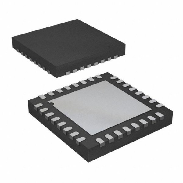
| Package / Case: | LFCSP-32 |
| Core: | ARM7TDMI |
| Program Memory Size: | 32 kB |
| Data Bus Width: | 32 bit/16 bit |
| ADC Resolution: | 24 bit |
| Maximum Clock Frequency: | 10.24 MHz |
| Number of I/Os: | 8 I/O |
| Data RAM Size: | 4 kB |
| Supply Voltage - Min: | 2.375 V |
| Supply Voltage - Max: | 2.625 V |
| Minimum Operating Temperature: | - 40 C |
| Maximum Operating Temperature: | + 125 C |
| Packaging: | Tray |
| Brand: | Analog Devices |
| Height: | 0.83 mm |
| Interface Type: | JTAG |
| Length: | 5 mm |
| Moisture Sensitive: | Yes |
| Number of ADC Channels: | 10 Channel |
| Number of Timers/Counters: | 4 Timer |
| Processor Series: | ARM7 |
| Product Type: | ARM Microcontrollers - MCU |
| Program Memory Type: | Flash |
| Factory Pack Quantity: | 1 |
| Subcategory: | Microcontrollers - MCU |
| Width: | 5 mm |
| Unit Weight: | 0.078802 oz |
♠ Low Power, Precision Analog Microcontroller, Dual Sigma-Delta ADCs, Flash/EE, ARM7TDMI
The ADuC7060/ADuC7061 series are fully integrated, 8 kSPS, 24-bit data acquisition systems incorporating high performance multichannel sigma-delta (Σ-Δ) analog-to-digital converters (ADCs), 16-bit/ 32-bit ARM7TDMI® MCU, and Flash/EE memory on a single chip.
The ADCs consist of a primary ADC with two differential pairs or four single-ended channels and an auxiliary ADC with up to seven channels. The ADCs operate in single-ended or differential input mode. A single-channel buffered voltage output DAC is available on chip. The DAC output range is programmable to one of four voltage ranges.
The devices operate from an on-chip oscillator and a PLL generating an internal high frequency clock up to 10.24 MHz. The microcontroller core is an ARM7TDMI, 16-bit/32-bit RISC machine offering up to 10 MIPS peak performance; 4 kB of SRAM and 32 kB of nonvolatile Flash/EE memory are provided on chip. The ARM7TDMI core views all memory and registers as a single linear array.
The ADuC7060/ADuC7061 contains four timers. Timer1 is a wake-up timer with the ability to bring the part out of power saving mode. Timer2 is configurable as a watchdog timer. A 16-bit PWM with six output channels is also provided. The ADuC7060/ ADuC7061 contains an advanced interrupt controller. The vectored interrupt controller (VIC) allows every interrupt to be assigned a priority level. It also supports nested interrupts to a maximum level of eight per IRQ and FIQ. When IRQ and FIQ interrupt sources are combined, a total of 16 nested interrupt levels is supported. On-chip factory firmware supports in-circuit serial download via the UART serial interface ports and nonintrusive emulation via the JTAG interface. The parts operate from 2.375 V to 2.625 V over an industrial temperature range of −40°C to +125°C.
Analog input/output
Dual (24-bit) ADCs
Single-ended and differential inputs
Programmable ADC output rate (4 Hz to 8 kHz)
Programmable digital filters
Built-in system calibration
Low power operation mode
Primary (24-bit) ADC channel
2 differential pairs or 4 single-ended channels
PGA (1 to 512) input stage
Selectable input range: ±2.34 mV to ±1.2 V
30 nV rms noise
Auxiliary (24-bit) ADC: 4 differential pairs or 7 singleended channels
On-chip precision reference (±10 ppm/°C)
Programmable sensor excitation current sources
200 μA to 2 mA current source range
Single 14-bit voltage output DAC
Microcontroller
ARM7TDMI core, 16-/32-bit RISC architecture
JTAG port supports code download and debug
Multiple clocking options
Memory
32 kB (16 kB × 16) Flash/EE memory, including 2 kB kernel
4 kB (1 kB × 32) SRAM
Tools
In-circuit download, JTAG based debug
Low cost, QuickStart™ development system
Communications interfaces
SPI interface (5 Mbps)
4-byte receive and transmit FIFOs
UART serial I/O and I
2C (master/slave)
On-chip peripherals
4× general-purpose (capture) timers including
Wake-up timer
Watchdog timer
Vectored interrupt controller for FIQ and IRQ
8 priority levels for each interrupt type
Interrupt on edge or level external pin inputs
16-bit, 6-channel PWM
General-purpose inputs/outputs
Up to 14 GPIO pins that are fully 3.3 V compliant
Power
AVDD/DVDD specified for 2.5 V (±5%)
Active mode: 2.74 mA (@ 640 kHz, ADC0 active)
10 mA (@ 10.24 MHz, both ADCs active)
Packages and temperature range
Fully specified for −40°C to +125°C operation
32-lead LFCSP (5 mm × 5 mm)
48-lead LFCSP and LQFP
Derivatives
32-lead LFCSP (ADuC7061)
48-lead LQFP and 48-lead LFCSP (ADuC7060)
Industrial automation and process control
Intelligent, precision sensing systems, 4 mA to 20 mA
loop-based smart sensors